## A New Pulse Battery Charger , by Jean-Michel Cour (France) http://www.theverylastpageoftheinternet.com/otherdevices/Cour/a_new_pulse_battery_charger.htm
# You can Charge a battery from any of these sources…
– Other battery (here: 12V lead/acid and 8.4 volt NiMH) – Solar Cell – AC Adapter
These do not allow for fluctuating and “undersized” power and voltage, but my humble pulse charger does.
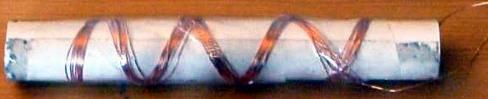
2″ X 4″ in size
This patent pending baby is based on a pulse charging technique similar to John Bedinis devices, but does not necessitate any timing adjustment.
# How it works:
The charger uses a step-charging section (left) to build up high voltage on an intermediate storage capacitor. An order of magnitude is x 2 the charged battery nominal voltage.
The discharge-on-voltage-threshold section (right) triggers discharge of the cap into the battery as soon as the predetermined high voltage has built up.
All details – including patent text and full replication advice (electronic diagrams, parts list ) are disclosed in this Yahoo Group: http://groups.yahoo.com/group/JMPulseCharger/
This is an open, unrestricted access Group. You are welcome. Just sign in and explore the messages, /files and /photos section
# Properties : The charger does not care fluctuating input (e.g. solar panel) thanks to the DC/DC cap charging technique that uses a step-up, inductive converter.
What will change is the time interval between cap discharges into the battery.
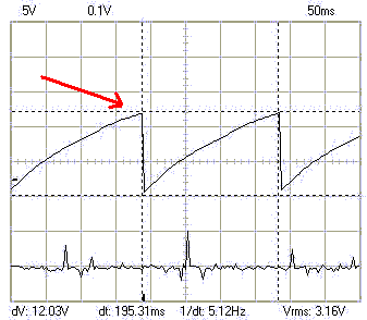
Here is a typical scope shot of the capacitor voltage waveform: the source was a small 7.5 volt rated solar panel, and the battery a small NiMH 8.4 volt rated battery. The threshold voltage (25 volt) is indicated by the arrow.
Overunity or not overunity ?
The inventor does not claim over-unity behaviour despite the similarity with John Bedinis description of pulse charging, but
-The charger shows abnormally better than expected performance vs. textbook theory (charge or energy switched through capacitor)
– It works even better if normal inductors are substituted a Caduceus coil with ferrite core
Want to know more ? Ask questions ? Email innodev2@wanadoo.fr ;Join http://groups.yahoo.com/group/JMPulseCharger/
Phone +33 1 64465442 ; Cell phone +33 6 15432229
## Method and apparatus of battery pulse charging allowing fluctuation of a DC current source
Invention domain:
The invention embodies a method and an apparatus specially suited for using a primary energy source that may exhibit slow or fast fluctuation of the available power.
It allows sourcing from various un-stabilized DC sources, allowing a constant quality of charging according to the technique of current impulses from a switched capacitor.
An application of special interest is when the source is composed of photovoltaic cells.
State of art
The method of energy transfer by means of a switched capacitor is not new. It is known since US patent # 685,858 by Nikola Tesla (November 5, 1901.)
According to this method, one awaits until an electric energy source has charged a capacitor up to a predetermined level for allowing this energy to be released to some load by means of a switch.
A bunch of methods exist as well for changing a DC voltage by means of transformers or switched capacitors, e.g. the Villard voltage multiplier. The devices using such methods are named DC/DC converters.
The provisional patent application US 2003/0117111 by John Bedini is based on a capacitor that is periodically charged up to a voltage greater than the battery rating from a source supposed to be a DC/DC converter, and pulse discharged into the battery.
In our understanding, this purely periodic method is not new in itself since it juxtaposes in an obvious fashion the cited Nikola Tesla invention and the well known process of charging a battery by means of periodic pulses.
Noticeably, Bedinis method foresee – according to his claim 1 – a characteristic step of disconnecting the capacitor from the source at the discharging stage, such step being unnecessary according to our invention.
Further, the periodicity of the capacitor discharge according to Bedini is not tolerant to substantial fluctuations of the source, whilst our invention is based on an a-periodic charging and discharge control method, which automatically adapts to said fluctuations.
DESCRIPTION
The present invention will be described using Fig. 1 to 4.
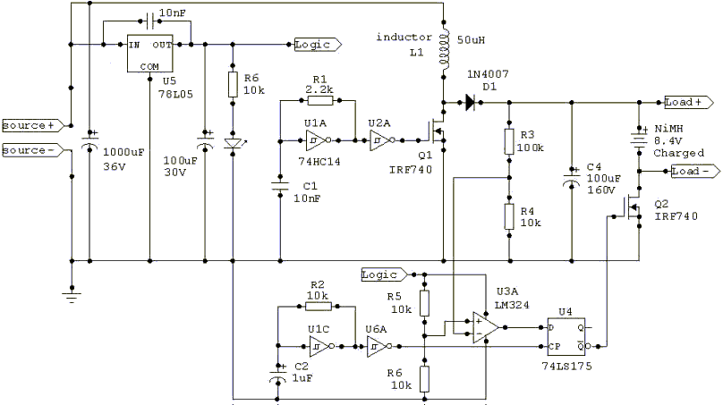
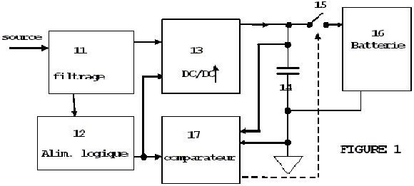
– Fig. 1 shows as block diagram a charger compliant with the invention, showing the capacitor step charging feature together with the comparator feature that triggers its discharge, which are the two essential parts of the invention.
– Fig. 2 is the full electronic diagram of an actual charger compliant with the invention, exhibiting the simplicity of implementation.
– Fig 3 is a timing diagram showing the self adaptation to the source fluctuations mechanism.
– Fig. 4 shows a variation of the Fig. 2 diagram where switching an only one resistor allows adjusting the capacitor discharge threshold depending of the battery type.
According to Fig. 1, a charger using the invention method is composed of :
– a filtering block (11) allowing a raw stabilization of a source that exhibits fast power fluctuations, such as a photovoltaic panel,
– a stabilized supply block (12) designed to power the charger control logic,
– a DC/DC converter stage (13) for step charging a storage capacitor (14) up to a predetermined energy level while tolerating the source fluctuations,
– a switch (15) for discharging the storage capacitor into the battery (16),
– a comparator device (17) controlling the 15 switch for discharging when the predetermined energy level is reached.
According to the invention, the source may exhibit substantial fluctuations without impairing the quality of the battery charge.
A first example of fluctuation can be changing the primary DC source.
So that the input of such a charger may be indifferently connected to:
– various battery types, in a wide range of voltage rating and capacity,
– various types of rectifying adapters from the grid AC, not necessarily stabilized,
– various types of photovoltaic cells.
Charging a battery from photovoltaic cells assembled into a solar panel isa specially advantageous application of the invention.
It is well known that a photovoltaic cell behaves as a constant current source under a given constant illumination, but actually exhibits significant fluctuations when illumination varies on the short or long term (time of day, orientation, atmosphere). The thereafter description will show how the charger reacts almost instantly to such available input power changes.
Fig 2 is the electronic diagram of a fully documented invention implementation, allowing sourcing from:
– any type of battery rated from some 5,6 volt up to more than 12 volt, or
– any grid AC rectifying adapter within the same voltage range,
– any photovoltaic panel that can fluctuate within the same voltage range,
provided the available power is sufficient to power the control logic.
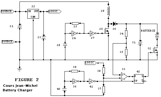
The raw filtering stage is made of an only one low voltage capacitor (21), under the only constraint of eliminating source disturbance too short to be absorbed by the logic supply or the DC/DC converting stage.
The logic power supply stage is made of anintegrated series regulator (22) of a known type designed for delivering a stabilized 5 volt potential to the control logic parts designed for this voltage (TTL and HCMOS technologies), and of a filtering capacitor (23).
Such filtering and supply stages are completely known and play a sole utility role in the invention.
The DC/DC conversion and step charging stage comprises:
– a RC oscillator based on a schmidt-trigger inverter (24) deliveringa symmetric clock signal which frequency is determined by the resistor (25)and the capacitor (26),
– another inverter (27) to buffer this clock and gate a switching, MOSFET type transistor (28),
– an inductor coil (29) that reacts to primary current cut-off by the 28 transistor under the form of high voltage pulses,
– a protecting and rectifying diode (30) allowing step ramp-charging of the storage capacitor (31) from the said high voltage pulses.
Generating high voltage pulses by switching off the current flowing into an inductor is in itself a well-known technique.
With the parts listed thereafter, the clock runs at some 65 kHz – not critical – and the voltage over the 31 capacitor could reach over 150 volt if it were not cyclically discharged into the battery by means of theMOSFET type transistor (32) acting as a switch.
The comparator stage embodies a differential amplifier (33) which inputs are polarized:
– on one hand, by the divider bridge made of resistors (34) and (35), reflecting the voltage over the 31 capacitor,
– on the other hand, by the resistors (36) and (37) acting as a half divider of the logic supply voltage i.e. 2,5 volt.
The 34 and 35 resistors values are so chosen:
– on one hand, as to not allow the voltage into the 33 amplifier input to exceed the supply potential (this could damage the circuit),
– on the other hand, to deliver a voltage slightly greater than the steady 2,5 volt reference voltage on the other input when the voltage over the storage capacitor exceeds a predetermined triggering threshold.
The switching transistor 32 gate control pulse is generated by means of another, sampling clock of the RC type, based on the schmidt-trigger inverter (38) which frequency is set by the resistor (39) and the capacitor (40). The signal of this clock is buffered by the inverter (41).
When the 33 comparator detects a crossing of the predetermined discharge voltage, a half period of this clock is latched by the Dflip/flop (42) which Q output gates the 32 transistor.
Using the chosen parts, the triggering clock as some 1 kHz frequency and therefore a 500 µs half period (not critical) , empirically determined as sufficient for discharging the storage capacitor down to the instant battery voltage.
As an example, a 25 volt triggering threshold order of magnitude has been empirically determined for charging a lead/acid, 12 volt nominal rated battery.
As evidence, this components are comon, of cheap cost and available from many sources:
– Filtration Capacitor 21 : 1000 µF 36 volt,
– Logic Tension Regulator 22 : IC 78L05,
– capacitor 23 to filtre the logic tension: 100 µF 36 volt,
– induction coil 29 : 50 µH,
– rectifying diode 30 : 1N4007,
– storage capacitor 31 : 100 µF 160 volt,
– inverters type «Schmidt’s trigger» 24, 27, 38 et 41 : four doors from one IC 74HC14,
– resistor 25 and capacitor 26 (charge oscillator) : 2,2 k ohm and 10 nF respectively,
– resistor 39 and capacitor 40 (pulse discharge) : 10 k ohm and 100 nF respectively,
– differencial amplificator comparator 33 : IC LM324,
– bascule « D » 42 : IC 74HC175,
– Power transistors MOSFET 28 et 32 : IRF740,
– resistors 34 et 35 to determine the switching level: 100 k ohm and 10 k ohm respectively,
– equal resistors 36 et 37 determine the reference potential: 10 k ohm.
The behaviour of the charger will be described with help of the Fig. 3 timing diagram, which shows a full operating cycle.
On this timing diagram the horizontal axis shows time, andvertically two signals:
– the voltage (301) over the storage capacitor (31),
– the gate control of discharge signal(302) out from the 43 D flip-flop.
Following an a-periodic cycle that begins after a capacitor discharge (time 310a), the storage capacitor is step ramp-charged until a variable time (310b) when the voltage exceeds the predetermined threshold (303).
This event is detected by the comparator, inducing the delivery of a switch gate control pulse (in fixed time 320a to 320b) during which the storage capacitor discharges itself, closing the cycle and starting a new cycle.
The charge time (310a to310b) is dependant on the instant power available from the source. Indeed, the process of producing high voltage pulses by current cut-off yields a per pulse voltage that directly depends on the switched off current according to the known dU = L x dI/dt formula. Therefore, the capacitor charging time depends directly on the available current.
In the case of sourcing from a photovoltaic cells panel exposed to the sun, it is known that the panel behaves as a current sourcealmost proportional to the incoming light flow. Therefore the capacitor charging time will in turn be variable and mostly proportional to the said light flow a the moment.
Conversely, the discharge pulse remains substantially stable as per its amplitude and duration. The top voltage built over the capacitor is slightly variable, with the sole uncertainty of the sampling clock period.
Therefore we have the desired characteristics,
– on one hand, of an automatic adaptation to the available power from a DC source submitted to large fluctuations,
– on the other hand, of a stable and free of source fluctuation charge quality thanks to the quasi constant discharge pulse calibration.
This is obtained through the invention characteristic of associating:
– a stage of voltage boost that ensures step charging of a storage capacitor,
– a comparator stage so designed as to trigger the said capacitor discharge toa battery as soon as the voltage reaches a threshold predetermined according to the battery type.
As described in the Fig 2 implementation example, the charger feeds a lead/acid, 12 volt nominal battery from a solar source designed for delivering around 14 volt under best lighting condition, as soon as this source provides a voltage of some 5,6 volt that is, enough to operate the control logic through the regulator.
Depending on the illumination, one will obtains full battery charge in a delay that adapts to the light flow variation including under such condition that would stall existing charges due to insufficient input voltage vs. the solar source expectation, thuswasting a significant part of the available energy.
It is possible as well to deliberately reduce the photovoltaic source power rating (cost per watt remains high) whenever much time is known to be available for charging a given battery, e.g. in heavily sun flowed countries where all day may be used for the purpose of night lighting.
If various types of batteries charging is desired (various technology, various voltage rating)it is enough to slightly modify the Fig.2 diagram by inserting (according to Fig. 4) a switch that allows to select as many threshold voltages by means of matching the 35a, 35b, 35c etc. resistors to each battery type or model.
According to this variation, the same above described charger will charge lead/acid, cadmium-nickel or NiMH technology batteries and various voltage ratings.Most known chargers do not exhibit this versatility because they are designed for a given battery type and voltage rating.
Skilled people will see evidence that sizing invention compliant chargers for various power ranges depends only on the appropriate sizing of:
– the filtering and storage capacitors,
– the switching transistors, or paralleling such transistors,
– the induction coil,
without questioning the control logic; the latter own power consumption will become more negligible according the overall charger power.
Skilled people may add such known add-on devices as :
– a charge limiter that disconnects the source as soon on upper battery voltage detection,
– thermal protection,
– state-of-charge indicators,
without leaving the invention domain.
Skilled people will see that, provided known caution measures, they may connect a load in-line with the battery without impairing the charger operation.
Moreover, contemplating the fact that the low start point of the charger operation only depends on enough power to feed the control logic, skilled people will envisage lower log standards e.g. the de facto 3,3 volt standard.This would allow solar charging from even lower illumination.
The logic could obviously be designed as an only one dedicated integrated circuit embodying the clocks generation together with the voltage over storage capacity comparator functionality, witha fixed or selectable threshold.
REVENDICATIONS
[ Claims wording is highly dependant on national/regional rules and traditions. No attempt is made of translating the claims into English a this early stage. The essentials of the claimed industrial property should be obvious from the above. ]
Contact the inventor: Jean-Michel Cour ; 35, Bd Dubreuil ; 91400 ORSAY ; France
(33) (0) 1 64 46 54 42 ; mobile phone (33) (0) 6 15 43 22 29 ; email innodev2@wanadoo.fr